Purpose
The RT8555 is a 36V High Efficiency Boost Converter with I2C Controlled 6-CH LED Driver. This document explains the function and use of the RT8555 evaluation board (EVB) and provides information to enable operation and modification of the evaluation board and circuit to suit individual requirements.
Introduction
General Product Information
The RT8555 is a high efficiency driver for white LEDs. It is suitable for single/two cell battery input to drive LED light bars which contains six strings in parallel and up to 10 WLEDs per string. The internal current sinks support a maximum of ±2% current mismatching for excellent brightness uniformity in each string of LEDs. To provide enough headroom for current sink operation, the Boost controller monitors the minimum voltage of the feedback pins and regulates an optimized output voltage for power efficiency.
The RT8555 has a wide input voltage operating range from 2.7V to 24V and contains I2C interface for controlling the
dimming mode, operating frequency and the LED current. The internal 100mΩ, 36V power switch with current-mode control provides over-current protection. The switching frequency of the RT8555 is adjustable from 300kHz to 2MHz, which allows flexibility between efficiency and component size.
The RT8555 is available in the WL-CSP-20B 1.65 x 2.05 (BSC), with pitch 0.4mm package.
Product Feature
-
Wide Operating Input Voltage : 2.7V to 24V
-
High Output Voltage : Up to 36V
-
Programmable Channel Current : 10mA to 35mA
-
Channel Current Regulation with Accuracy ±3% and Matching ±2%
-
Dimming Controls
►
Direct PWM Dimming up to 20kHz and Minimum On-Time to 400ns
► PWM to Analog Dimming up to 20kHz with 8-bit
-
I2C Programs LED Current, Switching Frequency, Dimming Mode
-
Switching Frequency : 300kHz to 2MHz
-
Current Limit, Over-Temperature Protection and Over-Voltage Protection
-
Input Under-Voltage Lockout
-
RoHS Compliant and Halogen Free
Key Performance Summary Table
|
Key Features
|
Evaluation Board Number : PCB025_V1
|
|
Default Input Voltage
|
3.8V
|
|
Default OVP
|
36V
|
|
Default Per Channel Output Current
|
20mA
|
|
Default Marking & Package Type
|
RT8555WSC, WL-CSP-20B 1.65 x 2.05 (BSC)
|
|
Operation Frequency
|
900kHz
|
|
Other Key Features
|
2.7V to 24V Input Voltage Range
Programmable LED Current, Switching Frequency, Dimming Mode
Output Over-Voltage Protection, Current Limit, Thermal Shutdown
20-Ball WL-CSP, with pitch 0.4mm Package
|
Bench Test Setup Conditions
Headers Description and Placement
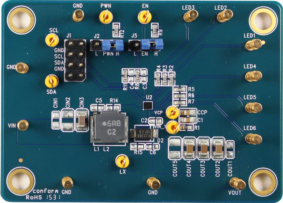
Please carefully inspect the EVB IC and external components, comparing them to the following Bill of Materials, to ensure that all components are installed and undamaged. If any components are missing or damaged during transportation, please contact the distributor or send e-mail to evb_service@richtek.com
Test Points
The EVB is provided with the test points and pin names listed in the table below..
|
Test point/
Pin name
|
Signal
|
Comment (expected waveforms or voltage levels on test points)
|
|
VIN
|
Input voltage
|
Boost conveter input voltage.
|
|
VIN_1
|
Input voltage
|
RT8555 VIN input voltage. Connected to VIN through R1.
|
|
VOUT
|
Output voltage
|
Output voltage up to 36V. Drive LED light bars by VOUT connect to FB1 ~ FB6.
|
|
LX
|
Switching node test point
|
LX waveform
|
|
EN
|
Enable input
|
Enable signal. Connecting this pin to pull high enable operation; floating this EN pin or connecting this pin to GND can disable the device.
|
|
PWM
|
PWM input
|
PWM Dimming Control Input.
|
|
FB1 ~ FB6
|
FB pin
|
Current Sink for LED1 ~ LED6. Drive LED light bars by VOUT connect to FB1 ~ FB6.
|
|
VCP
|
Internal regulator
|
LDO Output of Internal Regulator.
|
|
GND
|
Ground
|
Ground.
|
|
SDA
|
Data signal
|
Data Signal Input of I2C Interface.
|
|
SCL
|
Clock signal
|
Clock Signal Input of I2C Interface.
|
|
JP2
|
Chip enable control
|
Install jumper or drive EN directly to enable or disable operation.
|
|
JP5
|
PWM control
|
Install jumper or drive PWM signal directly to operation.
|
Power-up & Measurement Procedure
1. Connect input power and input ground to VIN and GND test pins respectively.
2. Connect LED ligh bars to VOUT and FB1 ~ FB6 test pins respectively.
3. There is a 3- pin header “EN” for enable control. To use a jumper at “H” option to tie EN test pin to input power VIN for enabling the device. Inversely, to use a jumper at “L” option to tie EN test pin and ground GND for disabling the device.
4. There is a 3- pin header “PWM” for PWM dimming control. To use a jumper at “H” option to tie PWM test pin to input power VIN for PWM = 100% dimming the device. Inversely, to use a jumper at “L” option to tie PWM test pin and ground GND for PWM = 0% dimming the device.
5. Usually use Function Generator to produce PWM signal to PWM dimming RT8555 ILED current.
6. Input PWM frequency about 200Hz ~ 20kHz.
7. For detailed RT8555 function operation, please reference RT8555 datasheet.
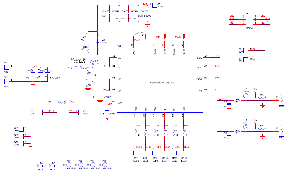
Schematic, Bill of Materials & Board Layout
EVB Schematic Diagram
Bill of Materials
|
Reference
|
Qty
|
Part number
|
Description
|
Package
|
Manufacture
|
|
U2
|
1
|
RT8555
|
LED Driver
|
WL-CSP-20B 1.65 x 2.05 (BSC)
|
RICHTEK
|
|
C1, CCP
|
1
|
C2012X7R1E105KT
|
1µF/50V/X7R
Ceramic Capacitor
|
0805
|
TDK
|
|
CIN3
|
1
|
GRM31CR71H475KA12L
|
4.7µF/50V/X7R
Ceramic Capacitor
|
1210
|
Murata
|
|
COUT2, COUT3, COUT4
|
3
|
UMK316BJ225KD-T
|
2.2µF/50V/X5R
Ceramic Capacitor
|
1206
|
TAIYO
|
|
D2
|
1
|
SR26
|
Schottky diodes
|
SMB/DO-214
|
PANJIT
|
|
L1
|
1
|
NR8040T6R8N
|
6.8μH/3.4A
DCR = 25mΩ, Inductor
|
L-NR8040
|
TAIYO
|
|
R1
|
1
|
|
10Ω/±1%, Resistor
|
0603
|
|
|
R2, R3, R4, R5, R6,
R7, R8, R9, R11, R12
|
10
|
|
0Ω, Resistor
|
0603
|
|
|
COUT1, CIN1,
CIN2, COUT5,
C2, C3, C4, C5, C6, L2, R14, R15
|
0
|
|
Not Installed
|
|
|
|
J1
|
1
|
|
4 x 2 Pin Header
|
|
|
|
J2, J5
|
2
|
|
3- Pin Header
|
|
|
|
TP1, TP2, TP3, Z3,
Z5, Z7, Z8
|
7
|
PWM, EN, LX, SDA,
SCL, VCP, VIN_1
|
Test Pin
|
|
|
|
GP1, GP2, GP3, GP4, GP5, GP6, GP7, GP8, GP9, GP10, GP11, GP12
|
12
|
VOUT, VIN, GND, LED1, LED2, LED3, LED4, LED5, LED6
|
Golden Pin
|
|
|
EVB Layout
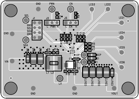
Top View (1st layer)
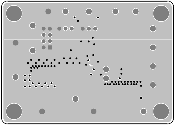
PCB Layout—Inner Side (2nd Layer)
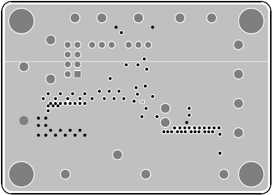
PCB Layout—Inner Side (3rd Layer)
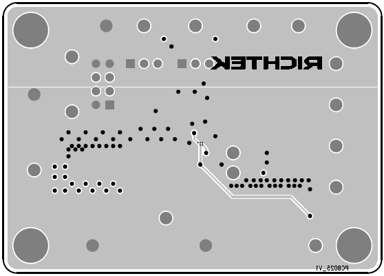
Bottom View (4th Layer)